I’ve had a very basic DAQ for thrust metering that needs to be connected to a PC. So I decided to make something more sophisticated and robust and most important standalone DAQ system for thrust metering…
When I designed the DAQ system I wanted it to have the following characteristics:
– 8 test capacity with 8 x 256 Kb memory banks
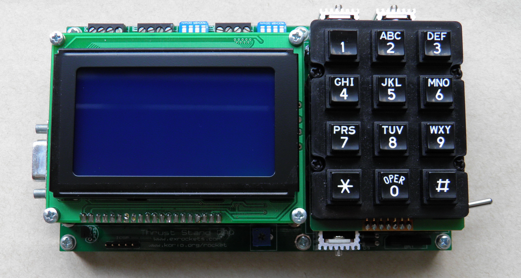
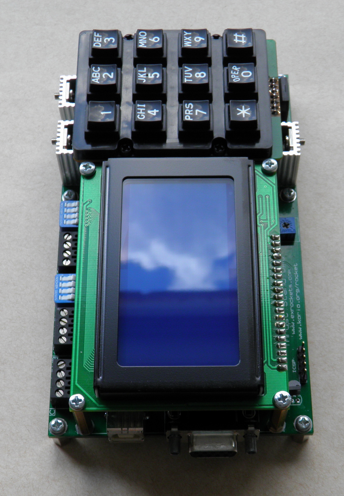
– 128×64 GLCD display
– Calculates test characteristics
– Displays test graph
– Keyboard
– Wide range power supply input (DC or AC from 5 to 18 volts)
– USB and Serial port for data transmission
– Temperature sensor
– 2 ports for load cell connection with selectable gain from 25 to 250 for each port
– 1 Port DC input from 0 to +5v with
– Audio signalization
– Standalone mode with 1000 (1 msec time interval) records per second or 16 seconds per test memory time for 1 port
– Real-time mode transmission to the PC with 100 (10 msec time interval) readings per second for all 3 ports
– 12 bit resolution ADC on MCU PIC18F4553
– +5v and -5v voltage reference
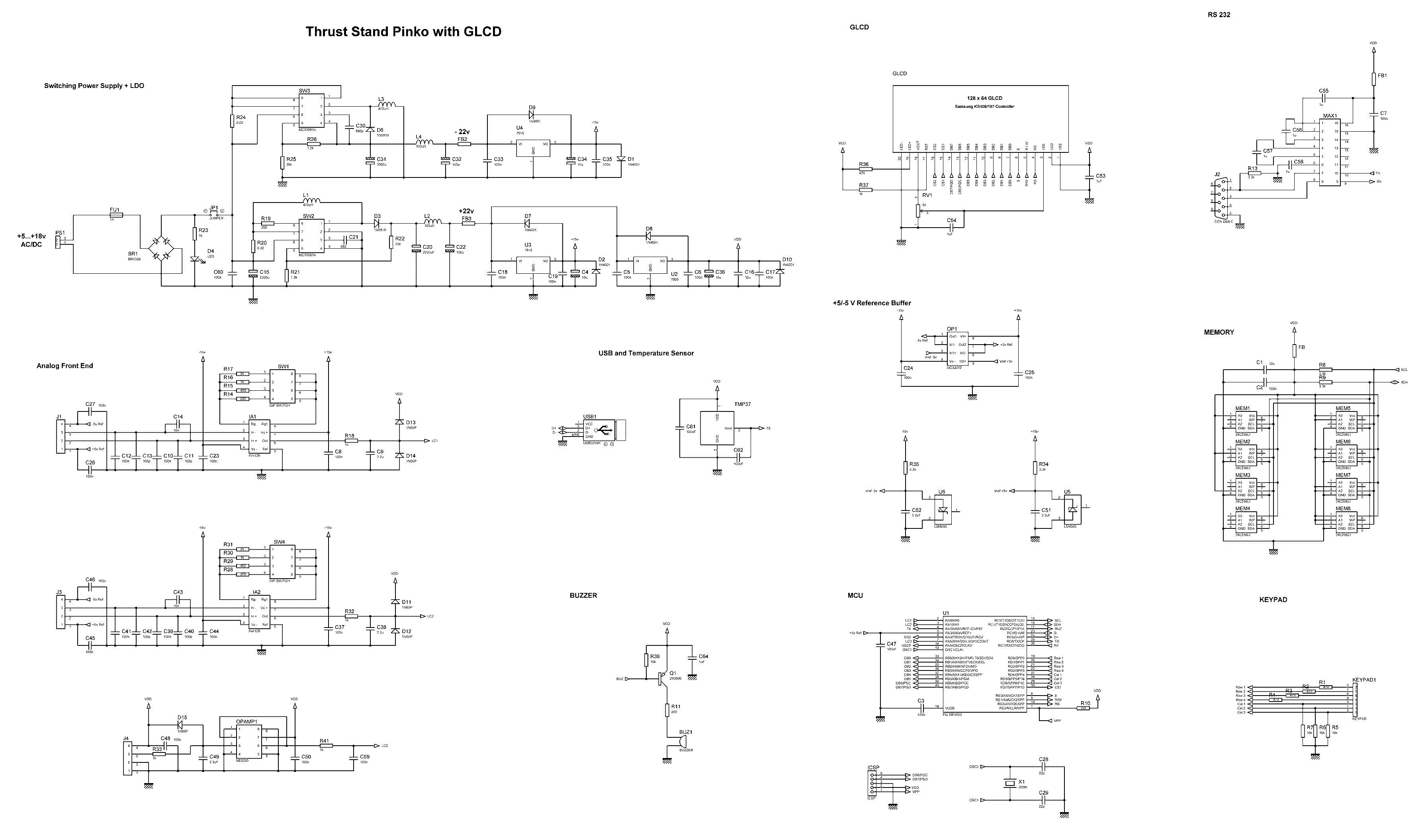
POWER SUPPLY:
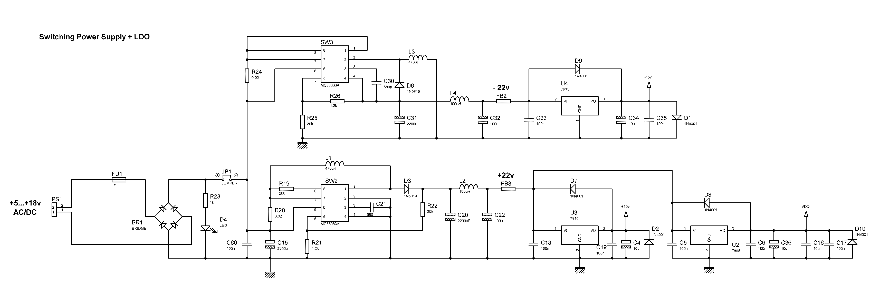
From the experience shared by other forum members it seemed that when using different power sources on the field for various reasons it happened to reverse the polarity. As result there was some damage on their DAQ systems therefore a diode bridge is the ideal solution if you don’t mind the voltage drop. With a diode bridge you can reverse the polarity, you can use DC or AC and it still will work.
Also I wanted to use a bipolar power supply for my DAQ system with wide range of voltage input. The best way to do it is to use a Switching Power supply. However the problem with switching power supplies is that they are noisy and can push some noise in the ADC. Therefore I put LC filters after the switching convertors and I used LDO regulators to get the desired regulated bipolar power supply of -15v and +15v needed for my Instrumental Amplifiers and voltage references. In addition there is a +5v regulator to power the digital part.
The power supply is protected with 1A fuse and in addition there are few discharge diodes to protect the ICs from damage if sudden power supply disruption occurs.
The end result is very robust power supply but quite energy inefficient because the switching regulators convert the input (3 to 18v AC or DC) to +21v and -21v and then the LDO regulators convert it to +15v, +5v and -15v. Thus there is large voltage drop mainly across the 7805 regulator that needs good heat sink actually it is best if all 3 LDO regulators have heat sinks. I am always using small motorcycle battery so energy consumption is not really a problem.
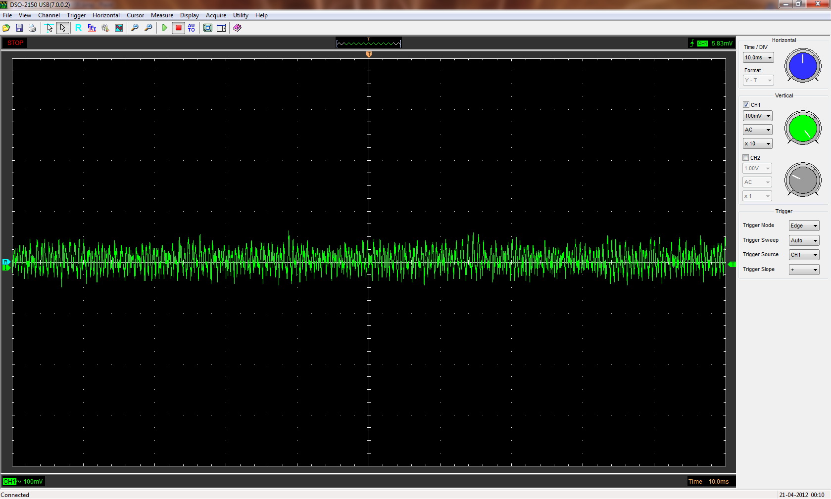
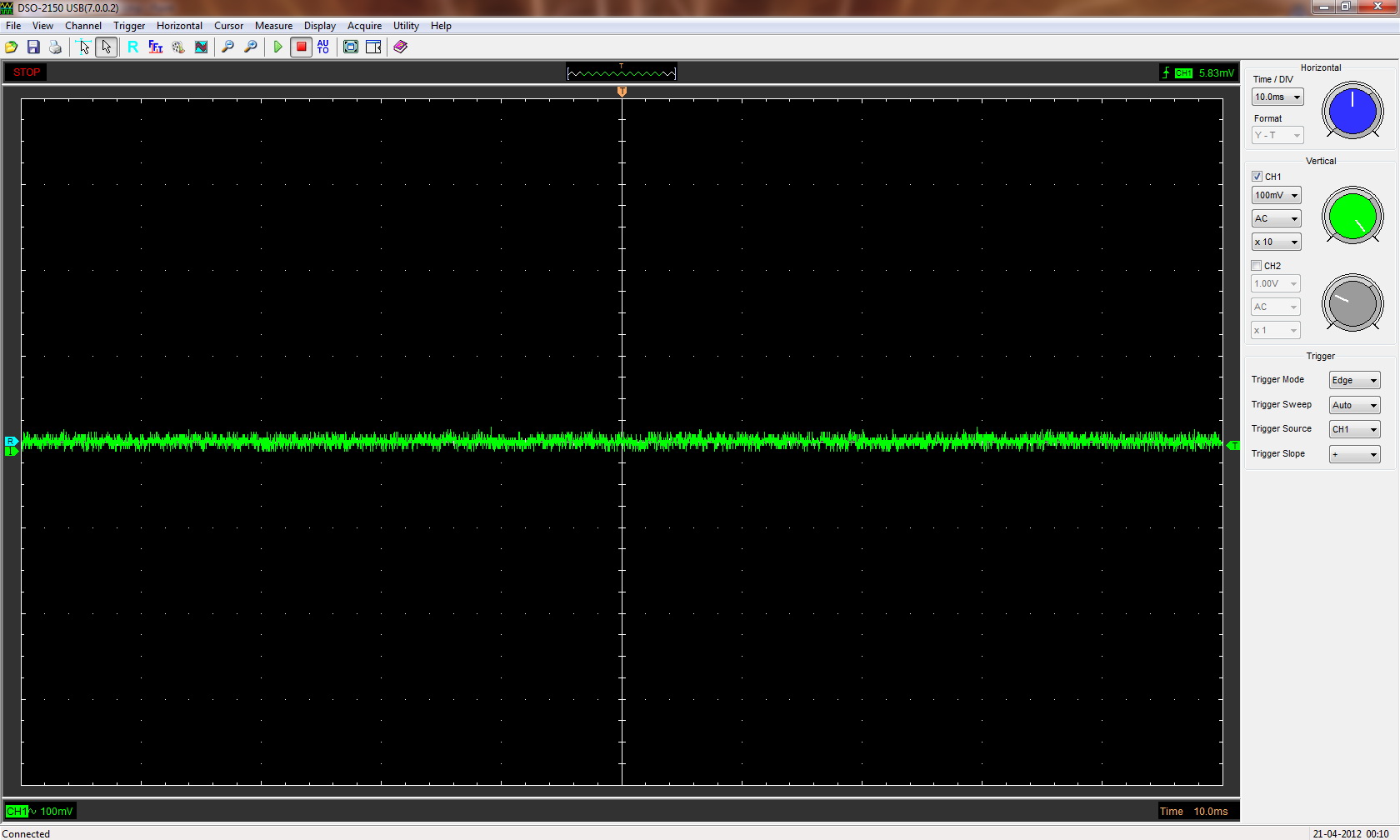
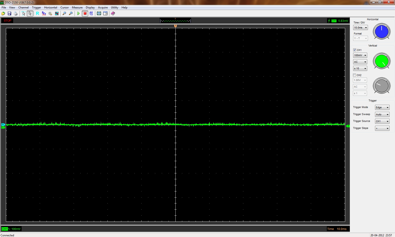
In terms of noise I took some measurements with my oscilloscope. Here’s how it looks like when the DAQ system is working:
The input power supply has significant voltage drops and spikes:
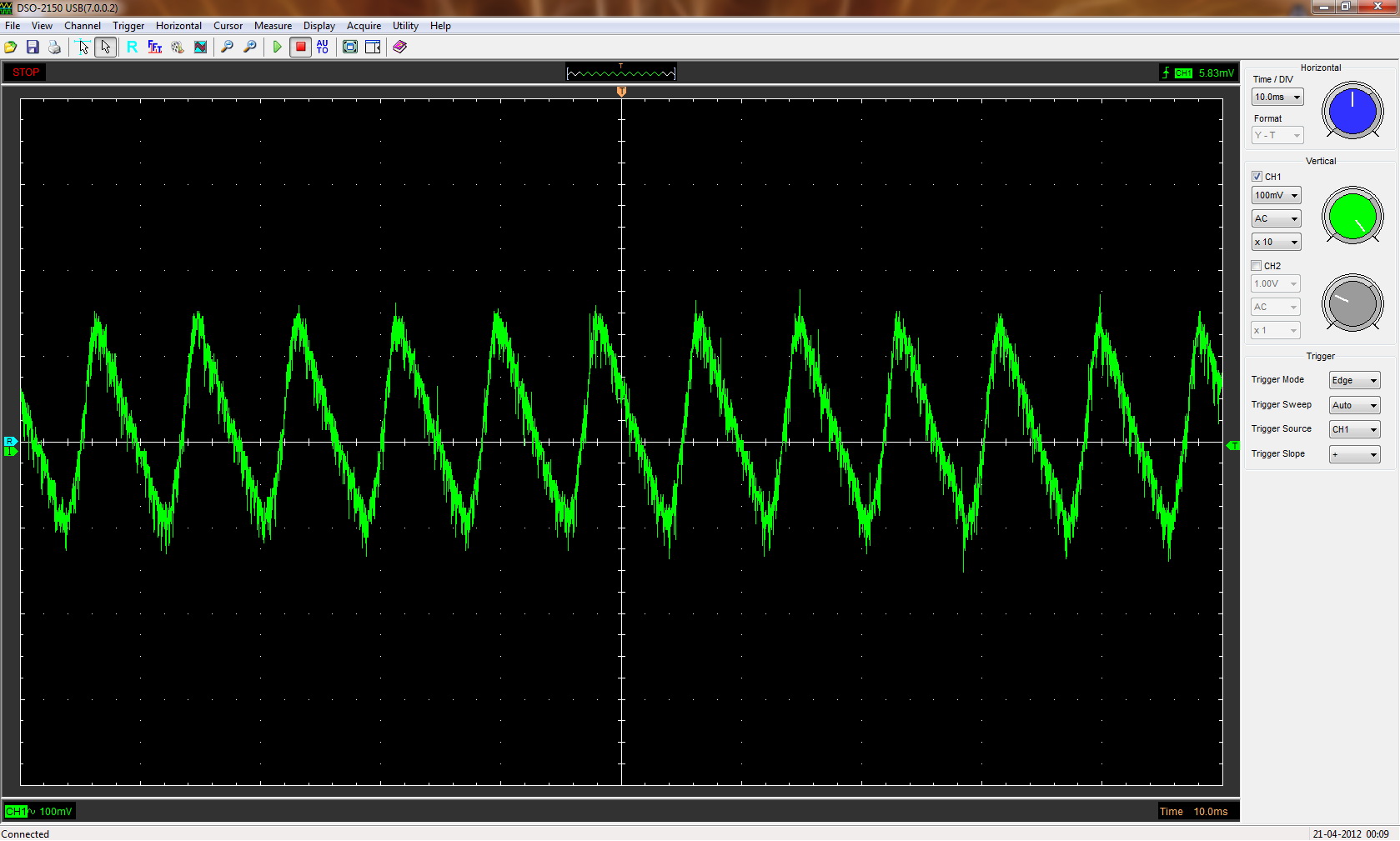
Then this is the filtered output from the switching supply, still some noise present:
And finally after the LDO the noise is minimal:
Just for reference my oscilloscope with grounded probe:
EDIT: I have updated the power supply schematic – D3 and D6 are now 1N5819 Schottky diodes as shown on the datasheet. It seems that this switching IC – MC33063A from TI – could become unstable as described here if you are using fast diodes (as I did) instead of Schottky type. However if you are using MC33063A from ON Semiconductor you might not have a problem with the fast diode, still it is best to be on the save side and use the 1N5819.
ANALOG FRONT END:
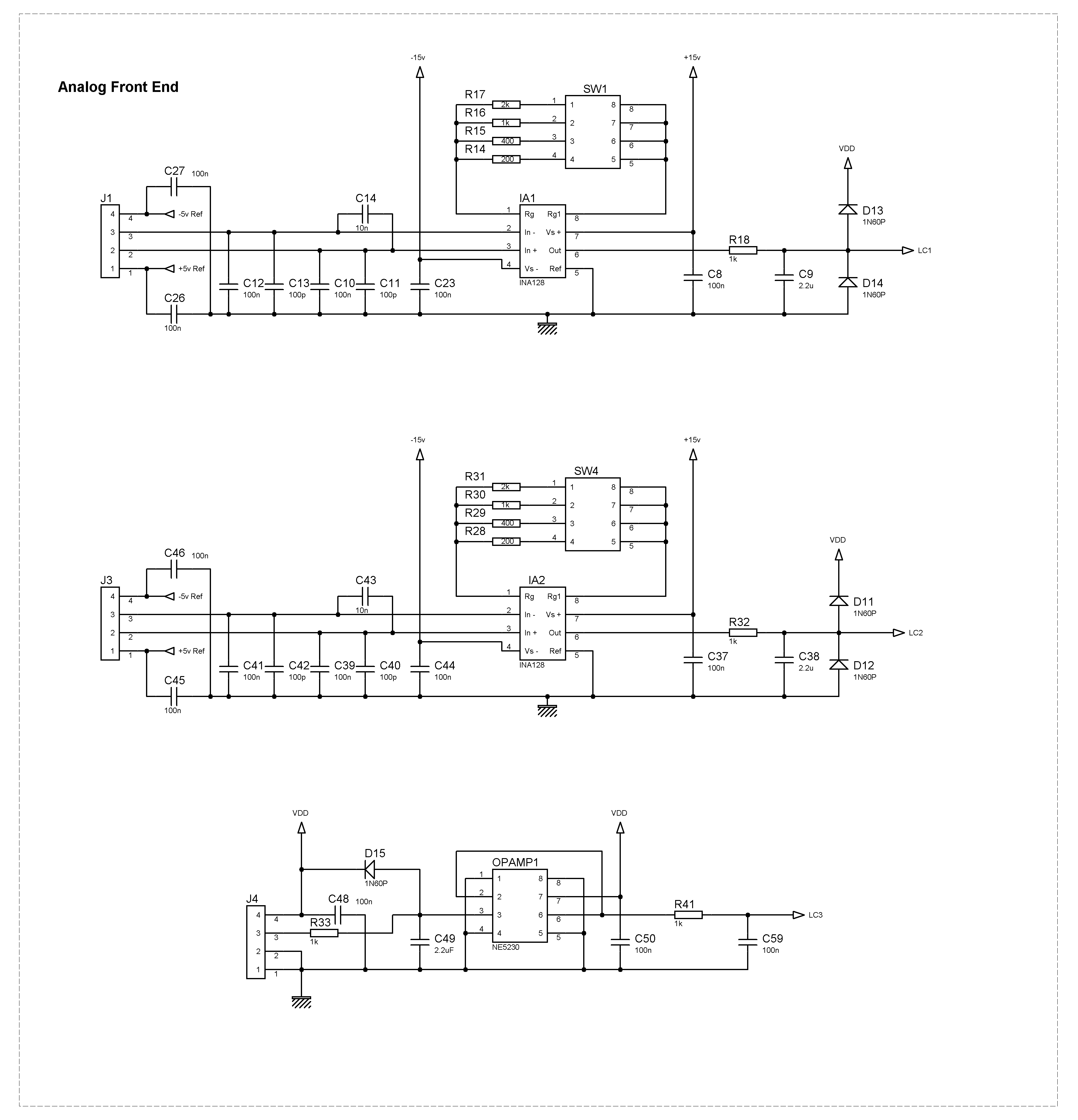
The analog part of my DAQ system has two inputs for load cells PORT A and PORT B. As Instrumental Amplifiers I am using INA128 which is a bi-polar amplifier. The gain can be selected through the DIP switch and the range with the selected resistors is from 25 to 250. With an output of 2mV/V for most load cells and 10v (-5v to +5v) supply that translates to a maximum output of 5V for the entire range. This is because the microcontroller’s ADC is unipolar and has range from 0 to +5v.
For example a 50kg load cell has an output of 2mV/V and the total power supply range is 10v thus 10V * 0.002V/V * 250 = 5v maximum output from the IA.
If you want to increase the resolution for given load cell you can cut the usable range by increasing the gain if you change the resistors.
For example a 50kg load cell has an output of 2mV/V and the total power supply range is 10v thus 10V * 0.002V/V * 250 = 5v maximum output. The ADC is 12 bit and converts this 5v reading to 2^12=4096 steps. That’s to say (50 kg)/(4096 bits) = 12.207 gr per bit.
Now say that you need higher resolution but you want to measure up to 25kg only. So you increase the gain to 500 (you have to change one of the gain resistors). What happens now: 50kg load cell has an output of 2mV/V and the total power supply range is 10v thus 10V * 0.002V/V * 500 = 10v maximum output from the IA. But the ADC accepts only up to 5 volts so the clamping diodes will limit the ADC input voltage to 5v. The ADC is 12 bit and converts this 5v reading to 2^12=4096 steps but this 5v corresponds now to 25kg only. That’s to say (25 kg)/(4096 bits) = 6.103 gr per bit. Everything above the 25kg will be shown as the maximum 25kg. So we lost half of the range but increased the resolution.
For the proper resistor values for selected gain see the INA128 datasheet.
As supply for the load cell I am using two 5v shunt voltage references (LM4040). The output of these references (+5v and -5v) is buffered through an OPAMP configured as voltage follower.
PORT C has no amplification and accepts signal input from 0 to +5v. This signal is buffered through a Rail-to-Rail OPAMP.
MEMORY:
The memory consists of 8 ICs x 256 Kb I2C memory. I am using 24C256LI from ON Semiconductors but any other compatible memory should do. Each memory bank holds 1 test.
KEYPAD:
The keypad specs: KEYPAD3X4
PC COMMUNICATION:
Communication with the PC could be established through either a USB or COM port. The COM port is buffered through an RS232 IC – I am using HIN232 but there are many compatible ICs and you can use any of them as long as they accept 115200 bps rate.
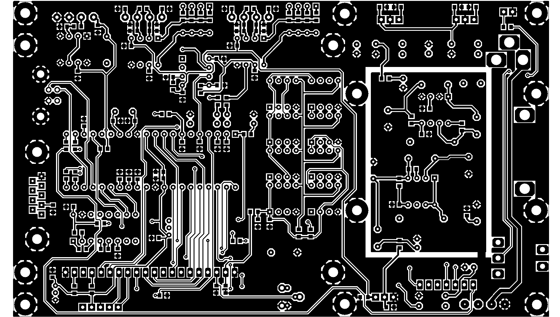
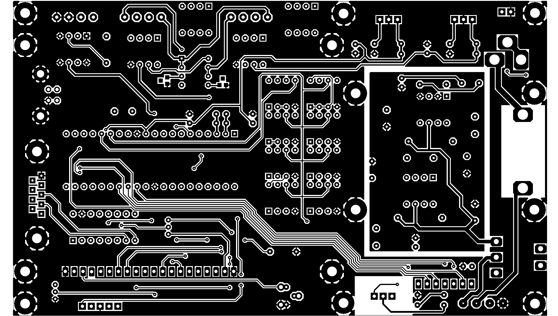
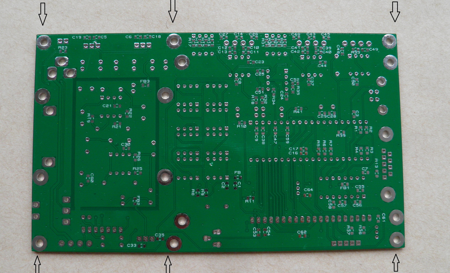
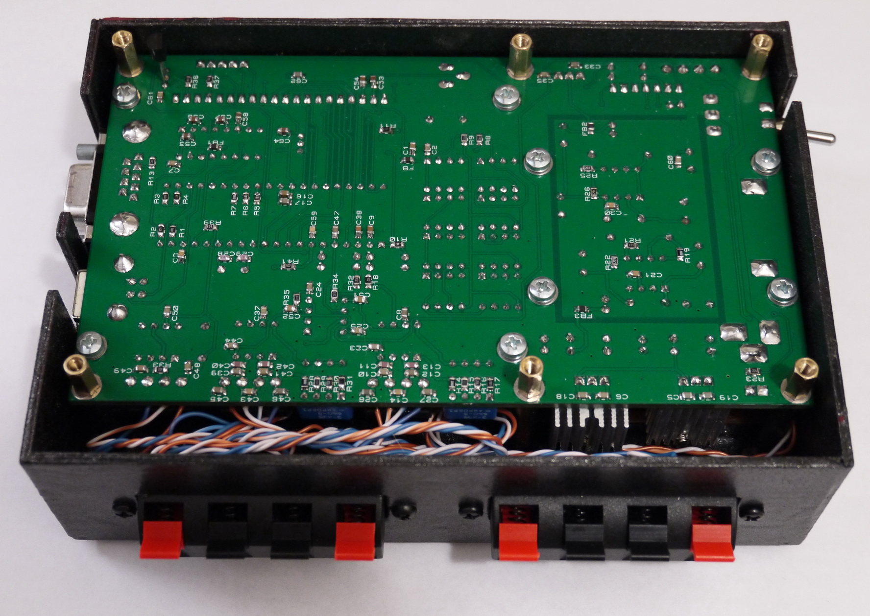
Next step is to prepare the PCB. Here’s how it looks like:
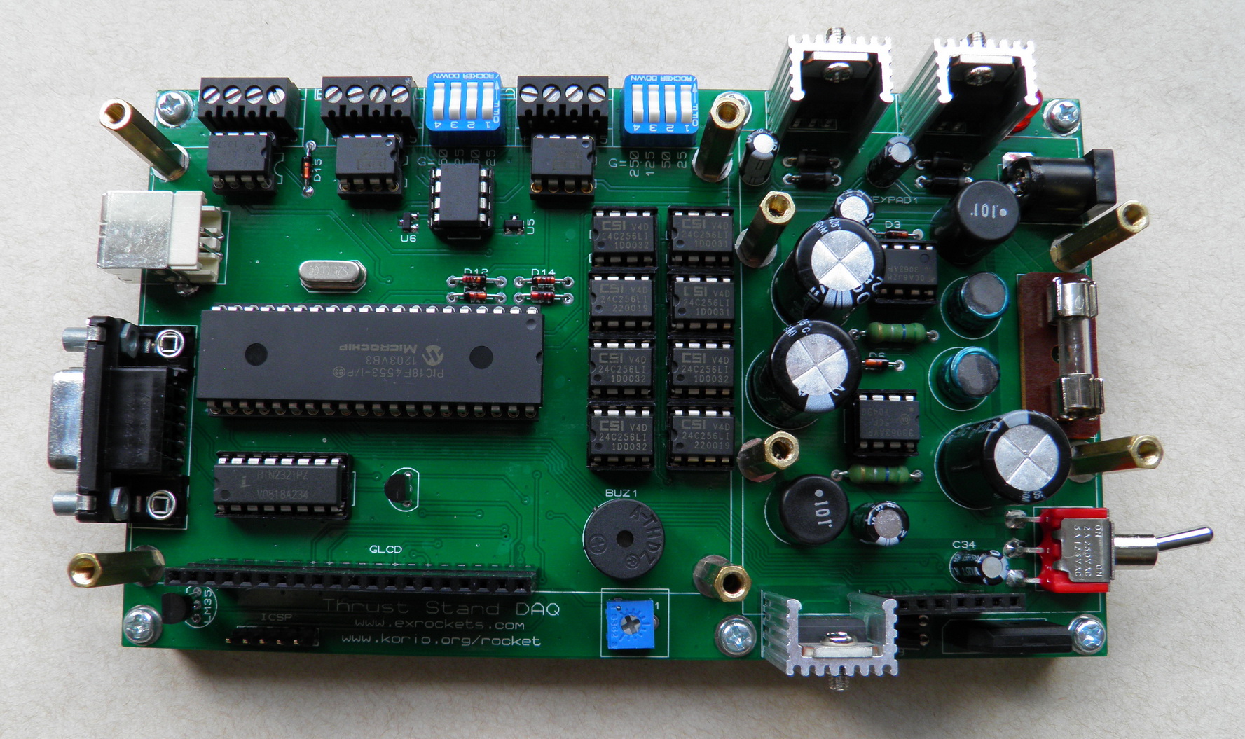
 Once I received the PCB it is time for assembly soldering (my favorite part):
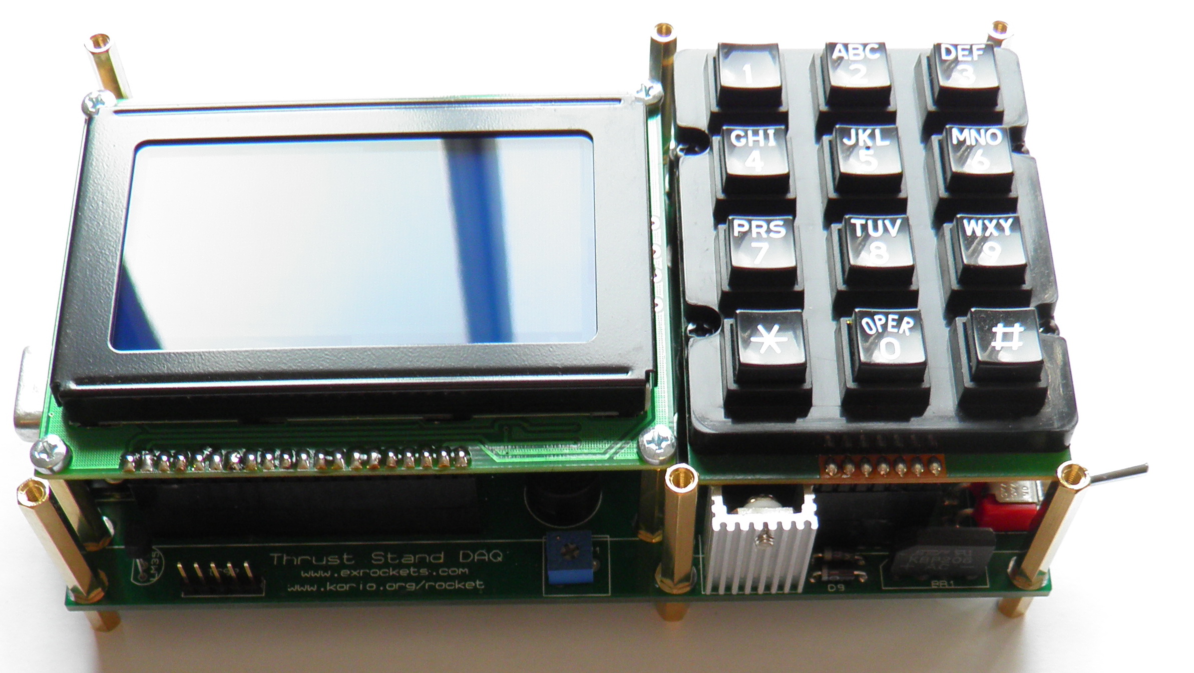
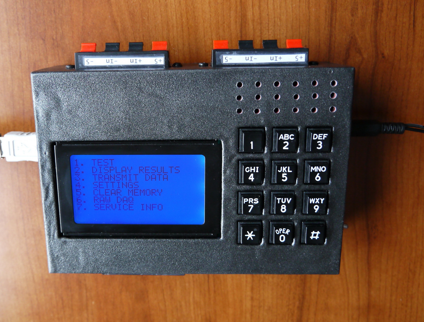
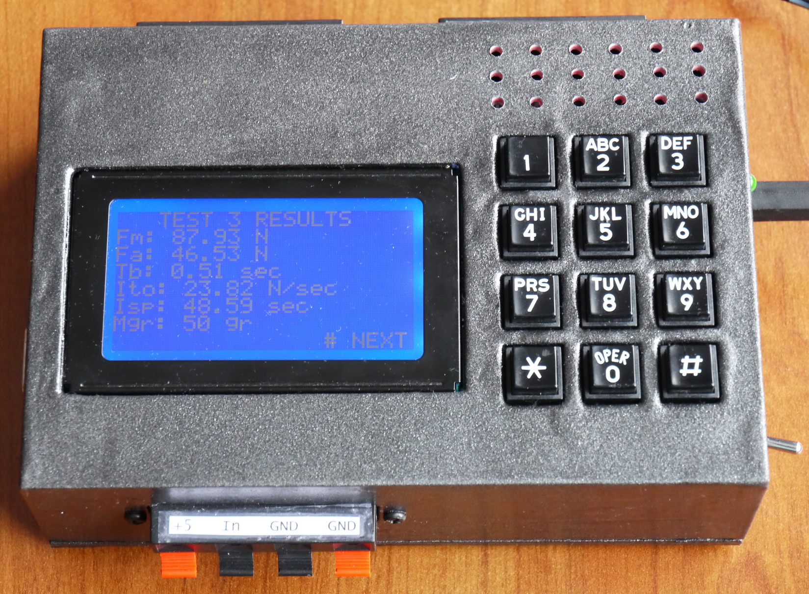
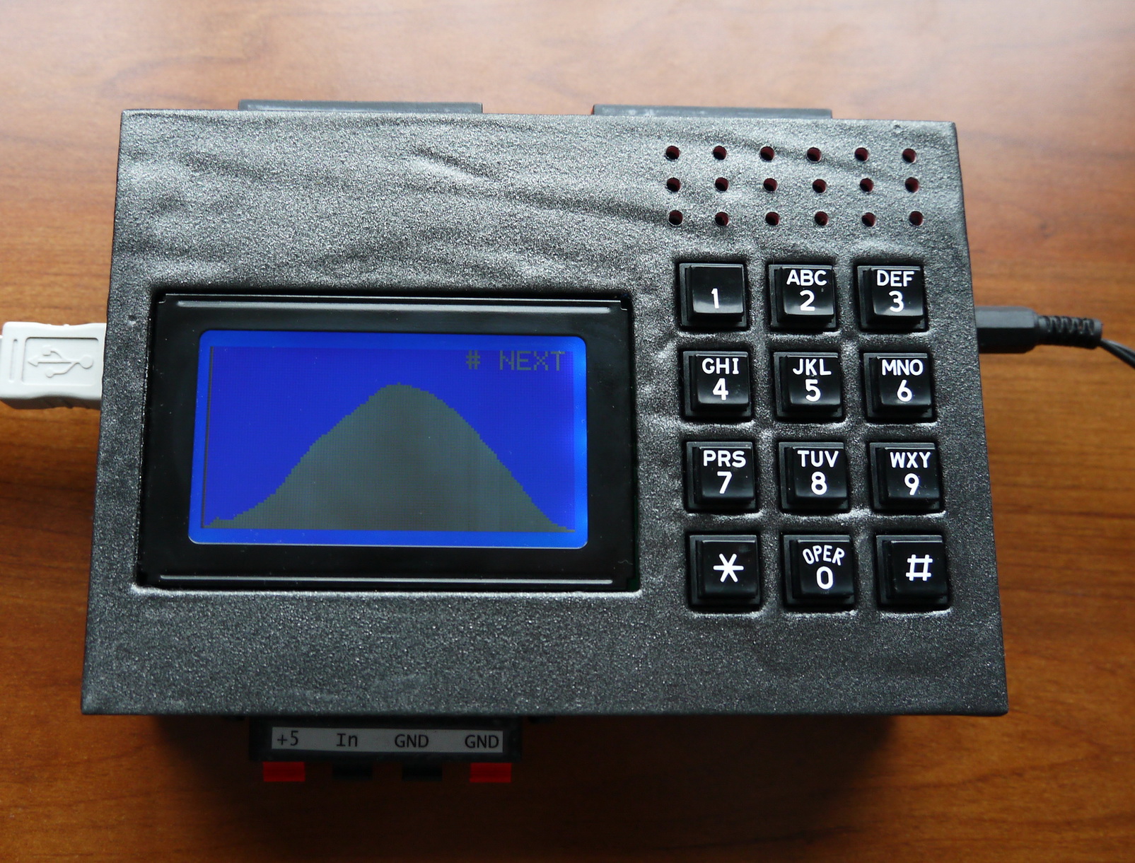
Once everything was assembled it was time to write the MCU firmware. Because I have many text menus the firmware took almost all of the MCU memory – near 95%. Anyway the DAQ system became quite functional for full description see DAQ MENU HELP.txt and here’s a short description:
– Records a motor test in standalone mode
– 8 selectable test positions
– Displays the test results
– Displays the test graph
– USB/RS232 output
– Sensor calibration
– Raw data transmission in real-time to the PC end
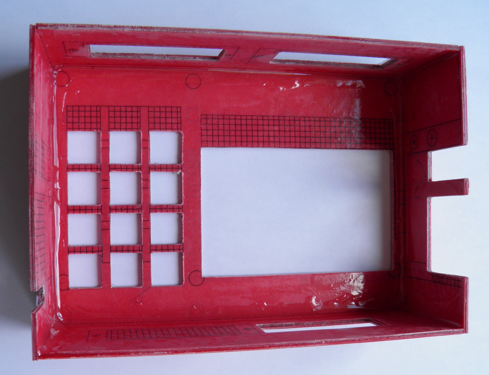
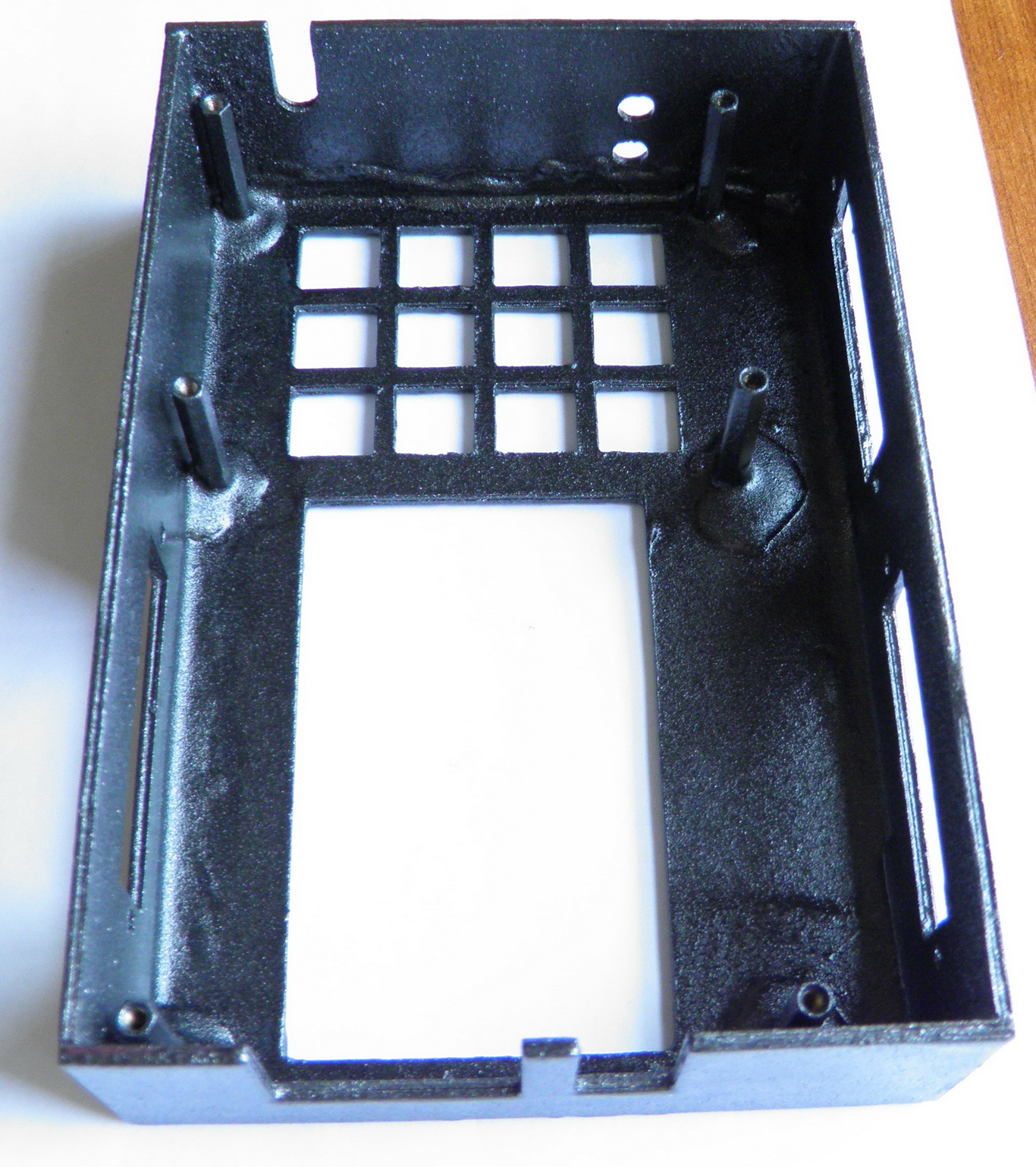
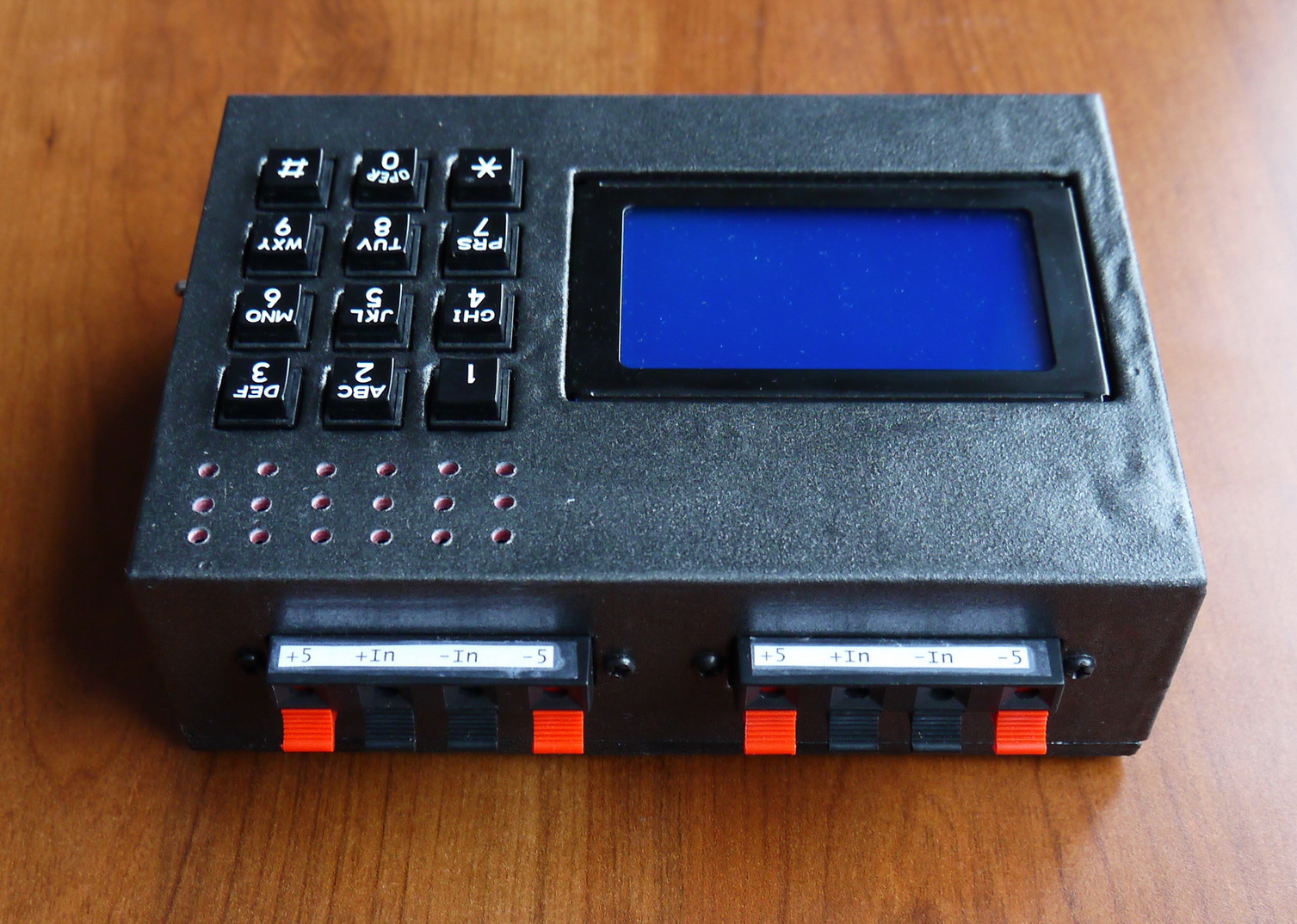
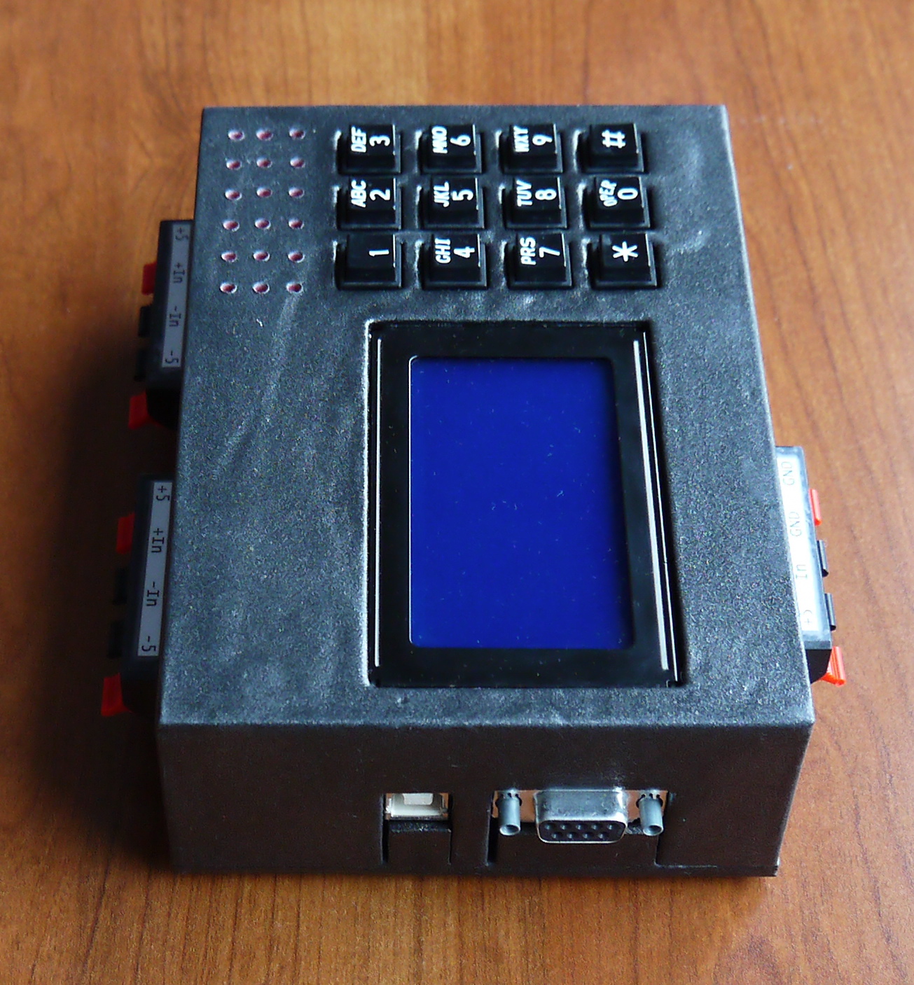
DAQ CASE:
Now when I finished the firmware the next thing on my mind was to find a suitable case. But after some looking I couldn’t find anything useful so I decided to make my own case. It would have been wonderful if I had access to 3D printer but I don’t have. The next best solution is to use get my hands dirty with some epoxy and make the case from thick paper and epoxy resin by epoxy laminating. The heaviest paper I found was 199 g/m2.

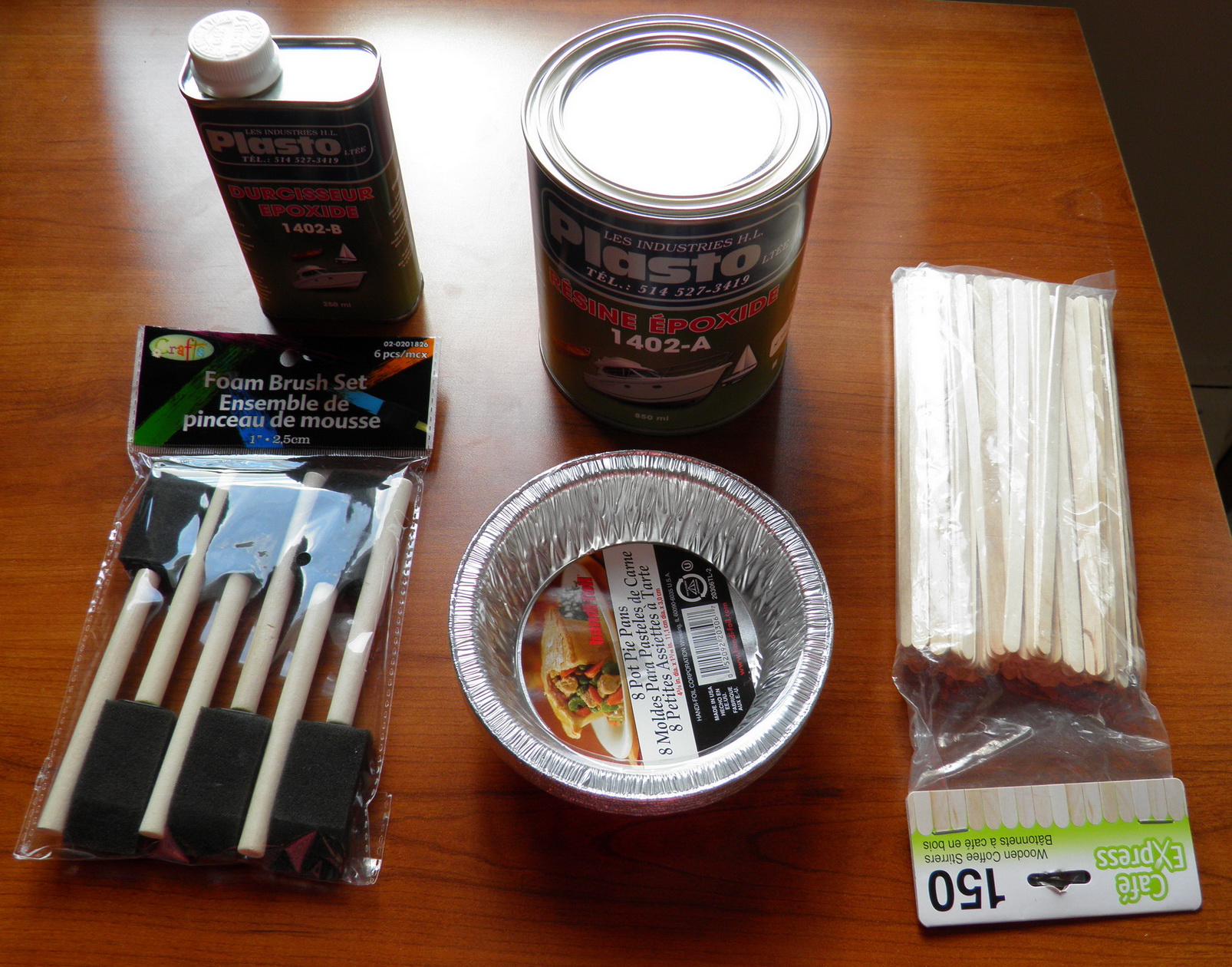
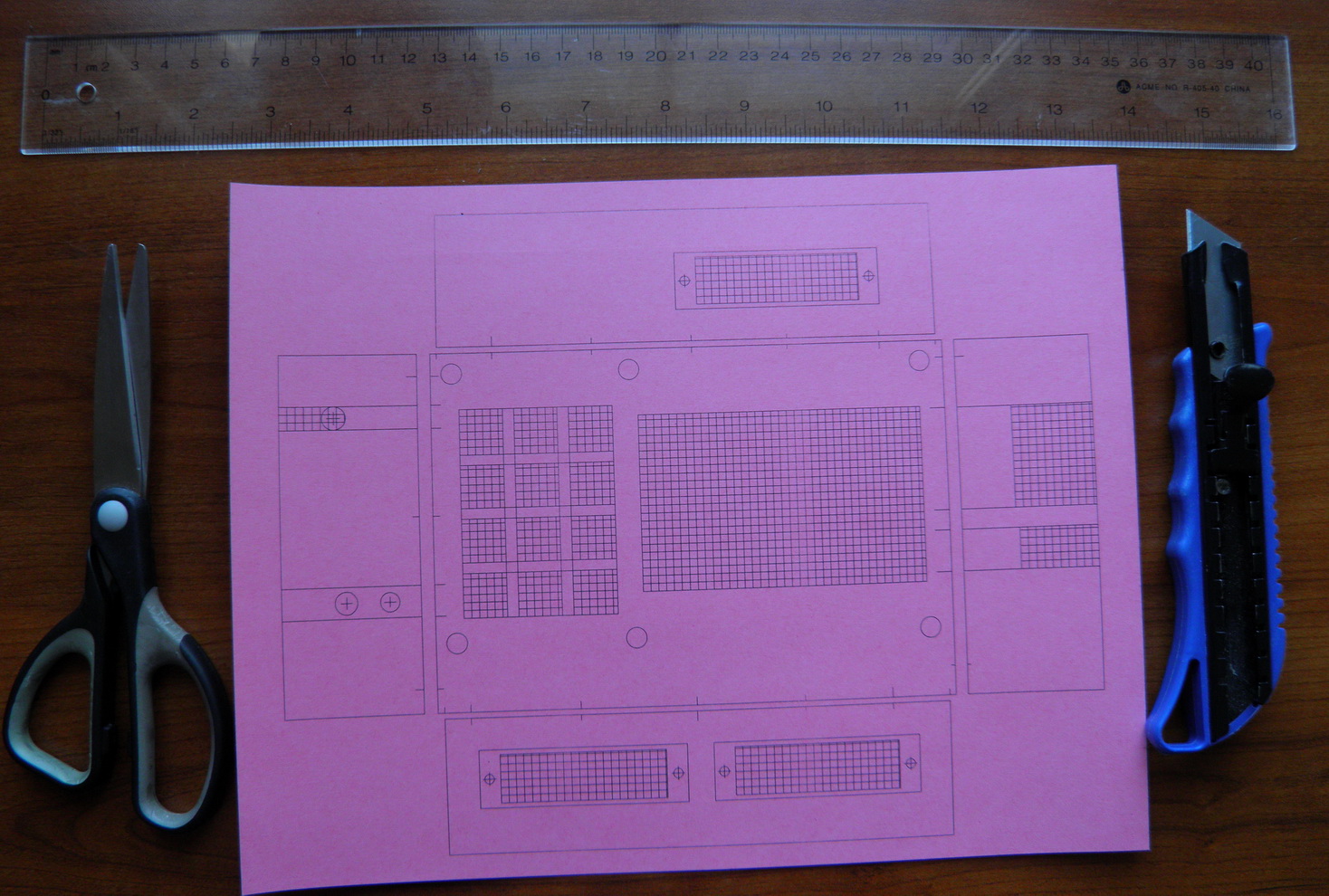
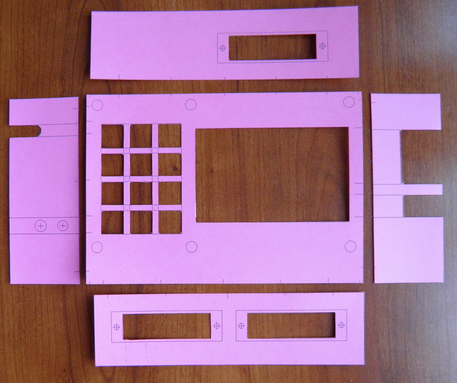
First step was to design the box and the drawings for printing. The drawings can be downloaded from here.
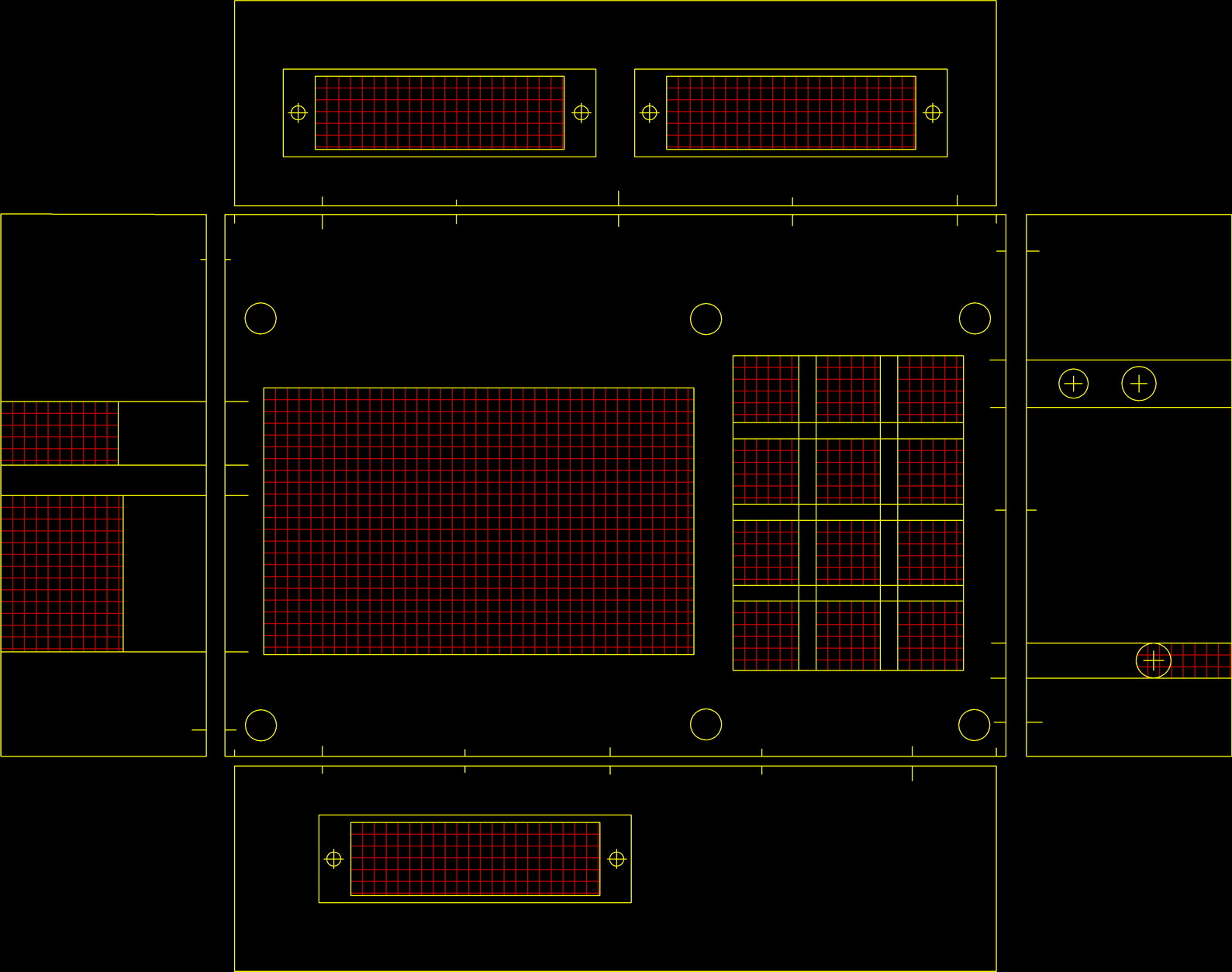
Second step was to print 10 pages and cut them out. I had some doubts if my laser printer would be able to handle the thick paper but it was no challenge for my old BROTHER HL-2140.
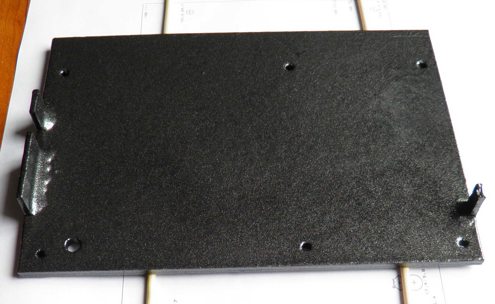
Third step is to laminate the paper and make the case walls.
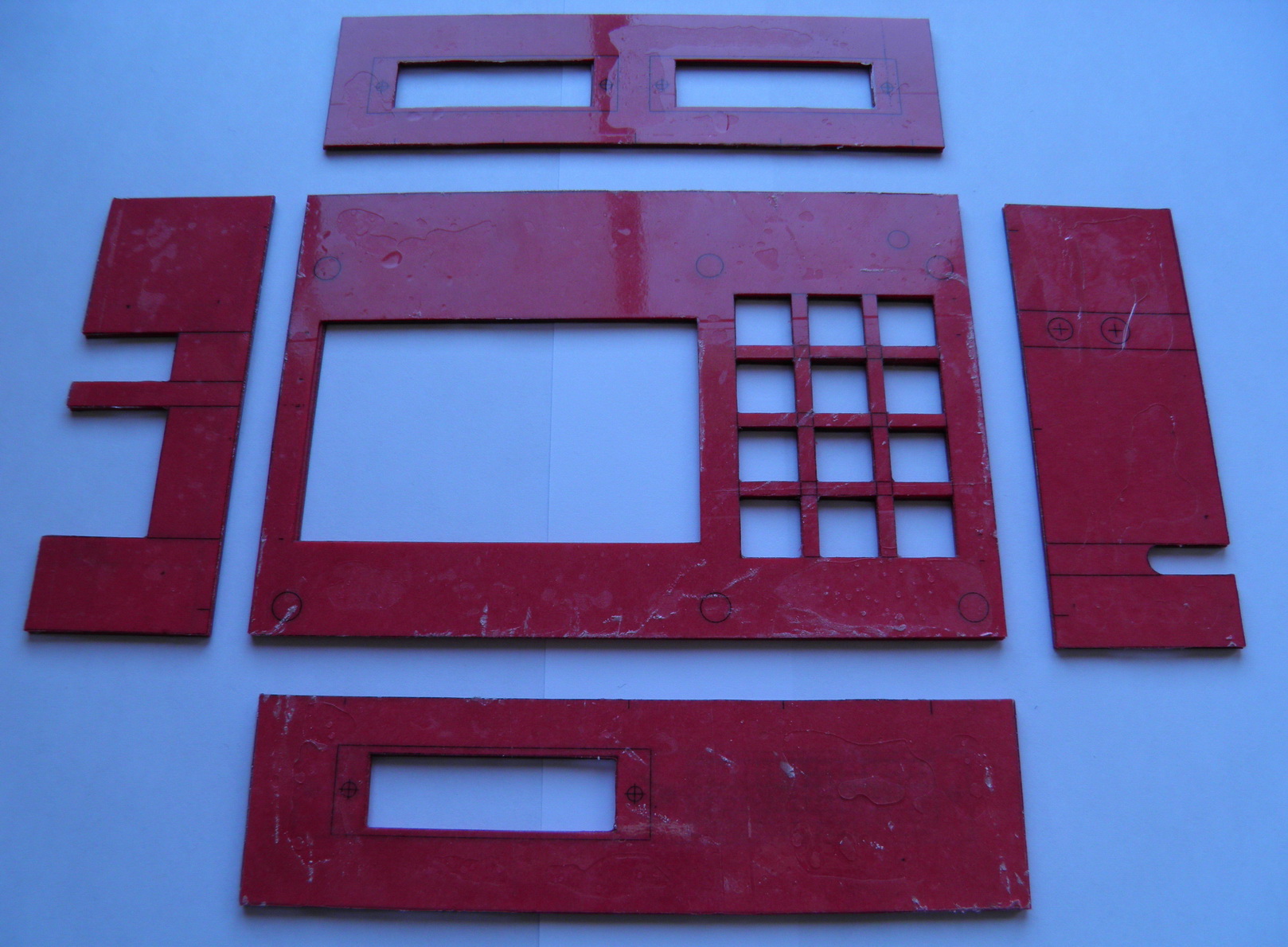
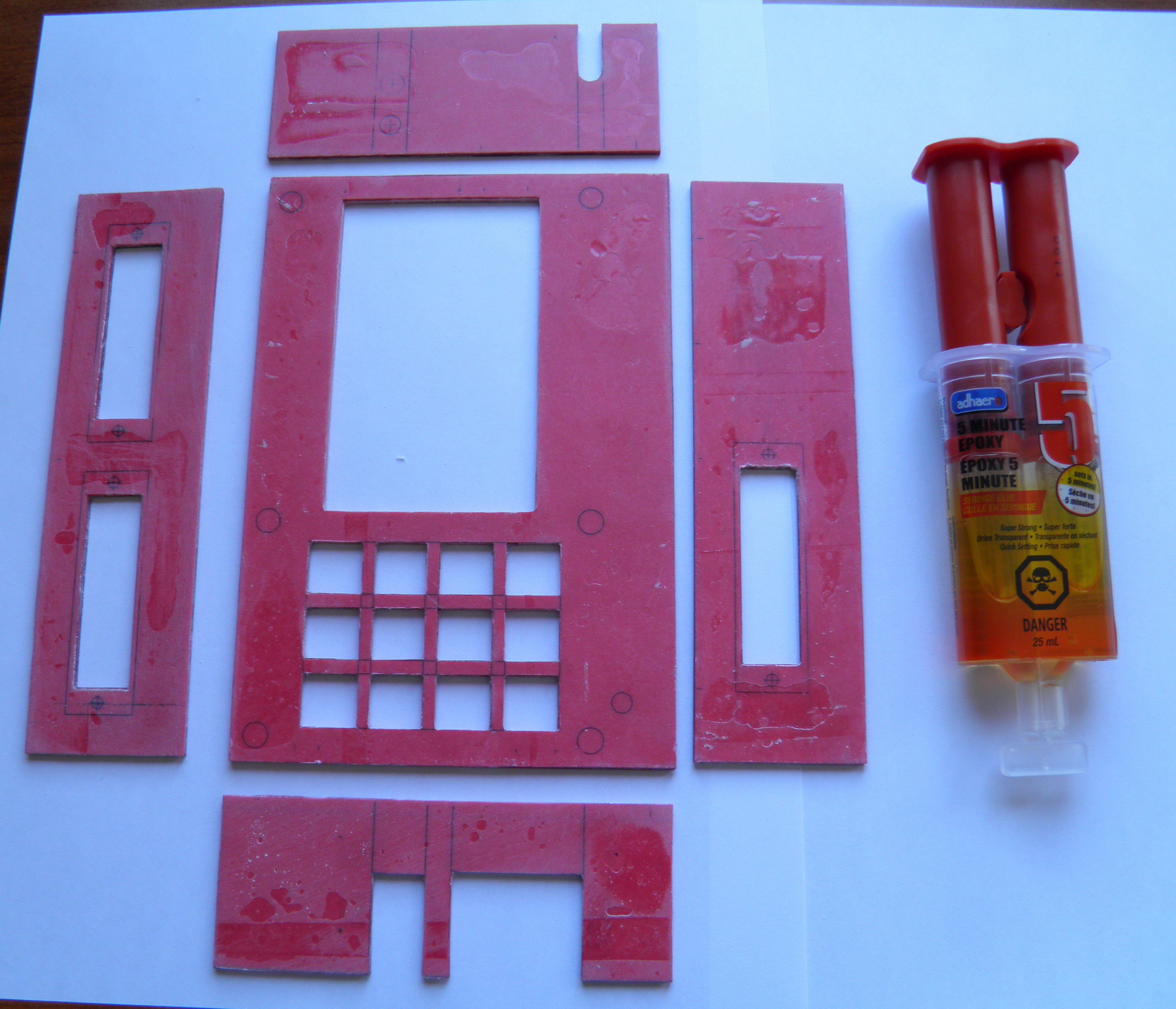
After the case walls cured out I did a little bit of sanding (I should have done a better work here, but didn’t have time that day) and it was time to assemble the case with 5 minute epoxy. First you fix the sides with tape on the outside and you put the rapid epoxy on the inside.
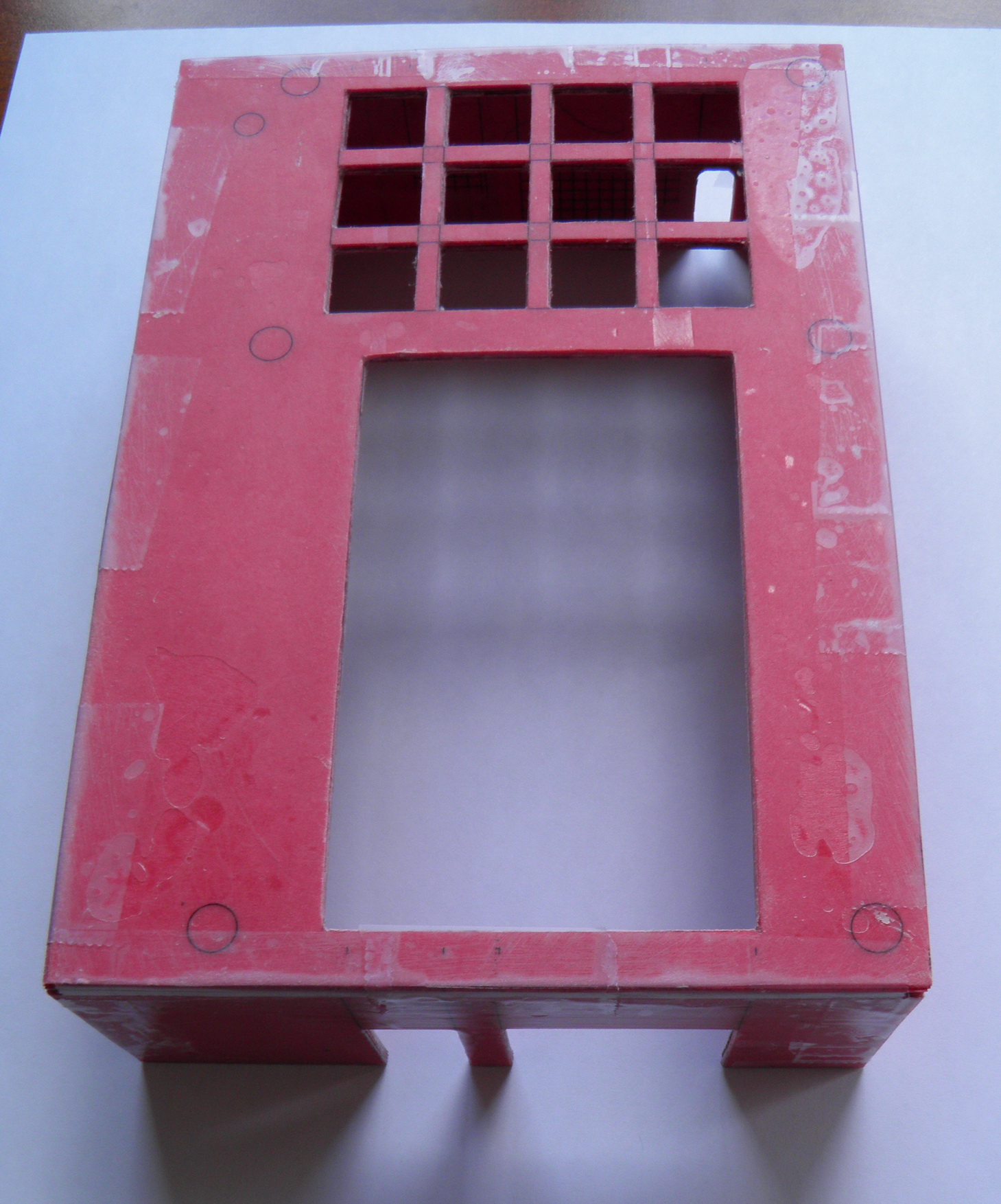
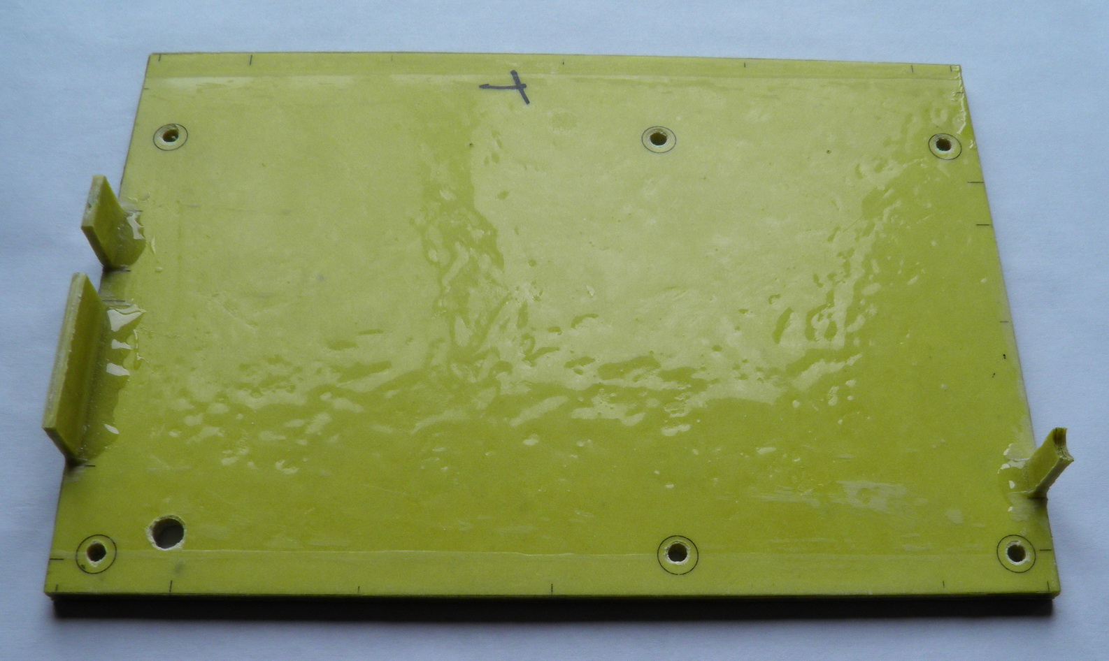
The same way I made the bottom side of the box.The LDO regulators create some heat and the temperature in the box can rise fast. To have accurate temperature readings the temperature sensor has to be insulated from the inside and to have good exposure to the outside air. Therefore I turned the sensor downwards (just soldered on the bottom side) and made a hole in the bottom left side of the box. The sensor goes in the hole and it is well exposed to the outside air.
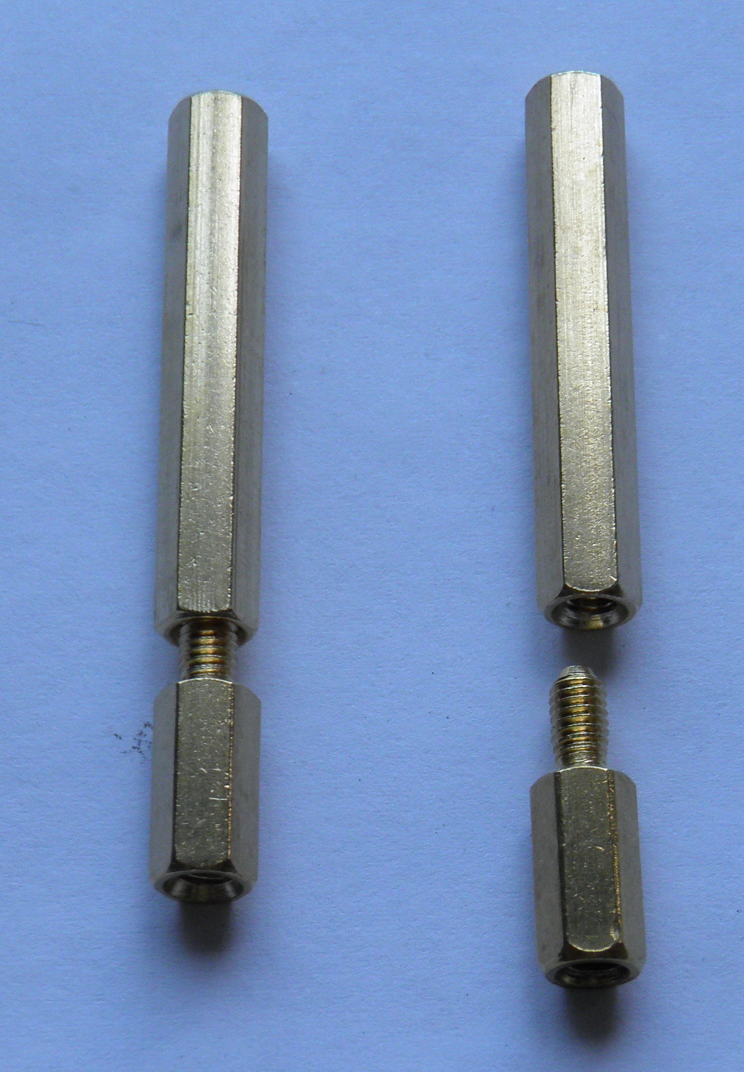
Once the case was ready I put the mounting brass standoffs inside the case and fasten them with the 5 minute epoxy.
Some painting work for humidity protection and better appearance.

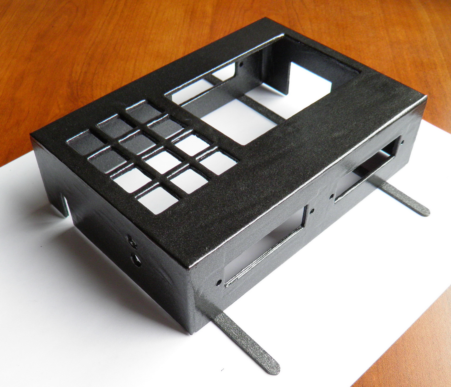
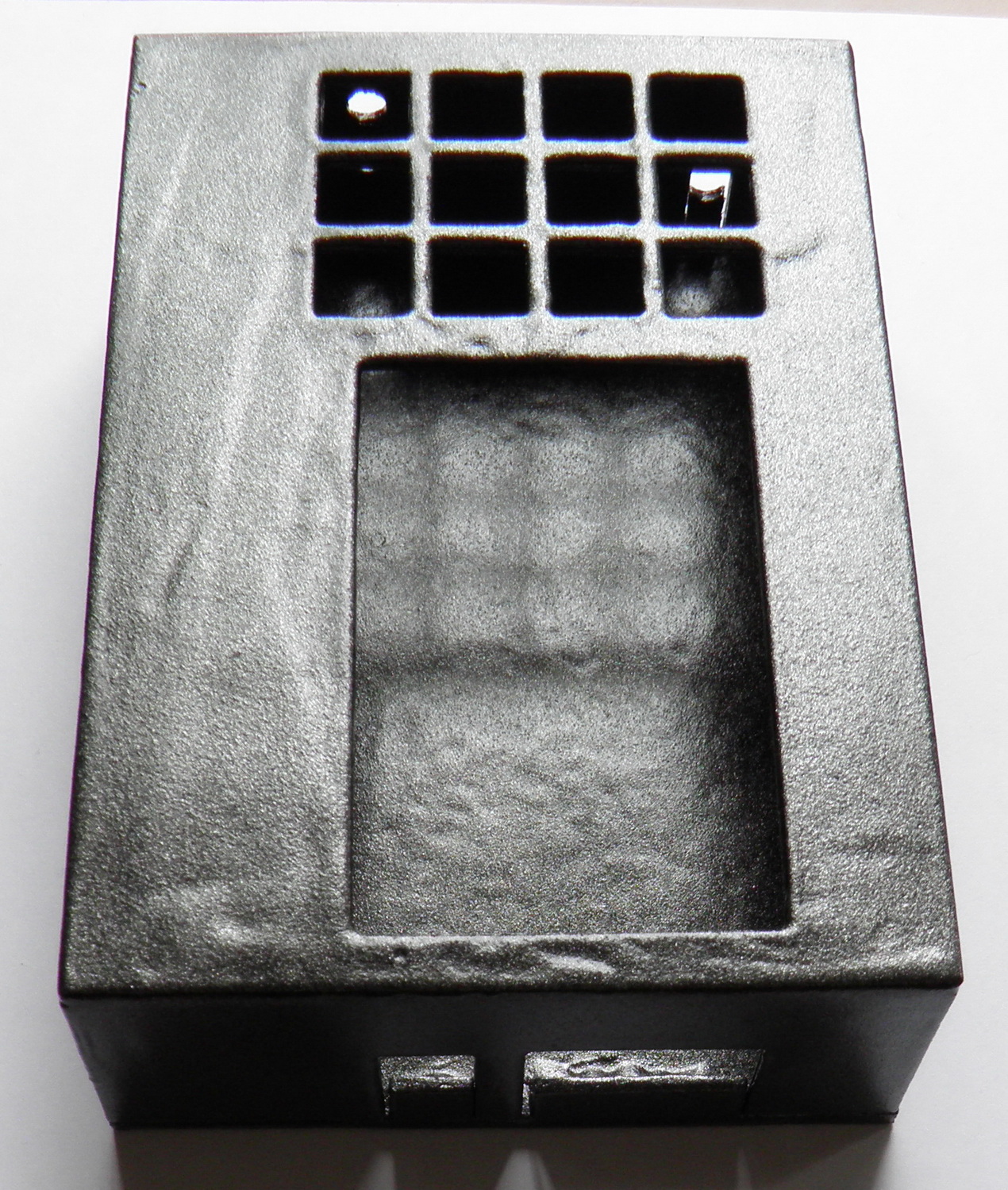
And finally I drilled several holes right above the heat sinks for better air ventilation. So this is how the empty case looks like and with the device inside.
PC APPLICATION:
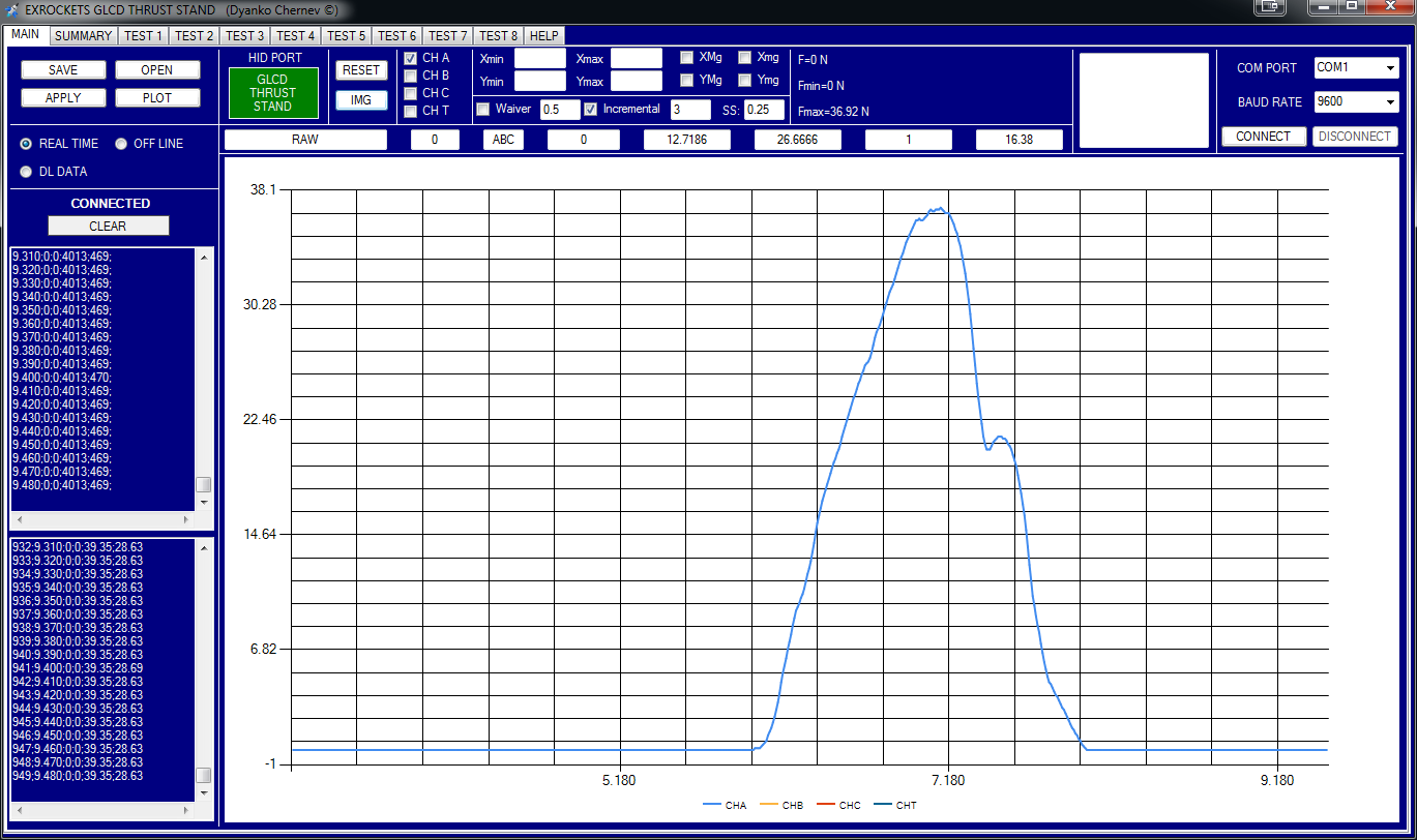
The last step was to make a PC application that will facilitate the DAQ – PC communication and in the same time it will crunch the data and visualize the thrust profile and test characteristics.
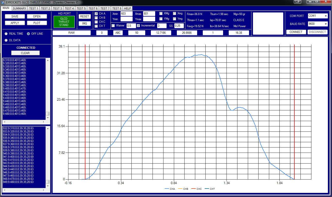
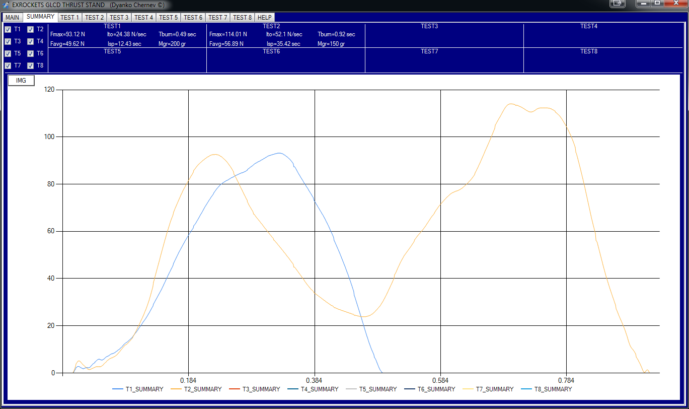
So the application allows you to download and save the test data, recalculate and visualize the test. Also you have the option to monitor and record the thrust in real time for all three ports. In addition you can compare the thrust profile for up to 8 tests. Full description is available in the HELP tab.
Real-time transmission and a dummy test:
The same test automatically recalculated only for the time interval of interest:
Here’s a second test opened with the program and how it compares with the first one:
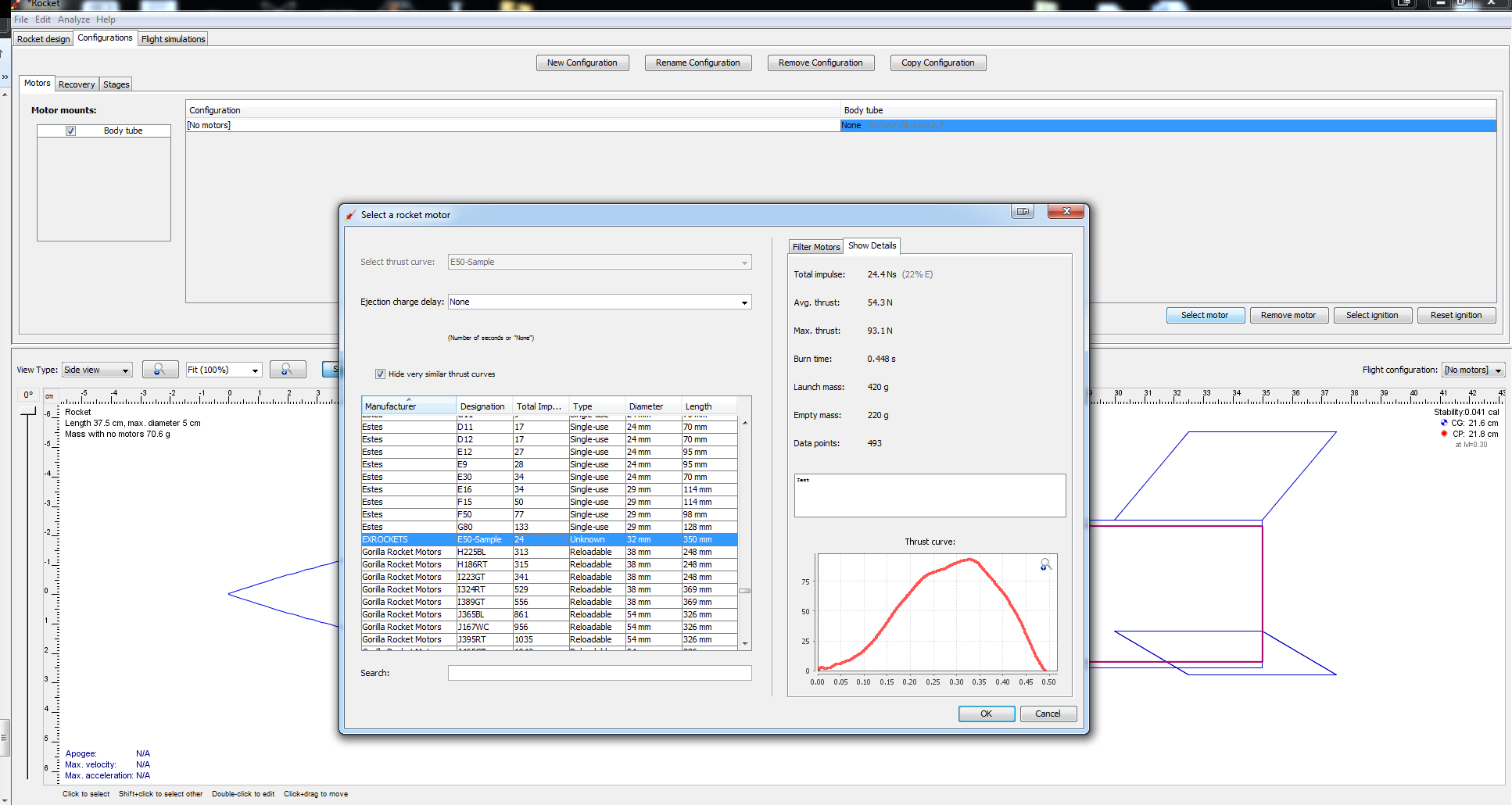
You can create also an ENG file which is the RockSim file format to hold the thrust and motor information and can be used in various programs like RockSim and OpenRocket.
If you want to use this application with other data sources you have to create a text file with the same structure as the one that the program uses, nothing really complicated.
– The program reads the file line by line
– Lines starting with an apostrophe (‘) will be ignored
– Data has 5 columns and is separated with semicolons (;)
– First line is data coefficients to convert the readings from the different ports.
Coefficients Port A and Port B are gr per bit, Port C is up to you, temperature
coefficients is bits per degree Celsius.
<Anything>;<coef Port A>;<coef Port B>;<coef Port C>;<coef Temperature>;
Example:
CH_Coef;12.461;26.7558;1;16.38;
– Second line is some test information, not really important but you
should have something
<Anything>;<Test ID Name>;<Test ID Number>;<Grain Weight>;<Triggering Port>;
Example:
Info;TEST-0U7;1;200;A;
– Next lines are test data
<Time in seconds>;<Bits Port A>;<Bits Port B>;<Bits Port C>;<Bits temperature>
Example:
0.000;0;0;0;498;
All together example:
‘GLCD THRUST STAND
‘*****************
CH_Coef;12.461;26.7558;1;16.38;
Info;GARGA-TS;2;150;A;
0.000;0;0;0;498;
0.001;5;0;0;498;
0.002;10;0;0;498;
0.003;16;0;0;498;
0.004;22;0;0;498;
0.005;32;0;0;498;
Firmware, PCB and PC application for this DAQ system.
GLCD_THRUST_STAND_APPLICATION 1.04
GLCD_THRUST_STAND_CADCAM_PCB_FILES
GLCD_THRUST_STAND_HID_FIRMWARE 1.06
Leave a Reply